It occurred to me today that I had not written a blog post about Circuit Board Design yet! It's one of the most interesting topics for people that don't practice electronics weekly because it lets them see what's inside their technology and how it was designed, it tends to give people a better appreciation of the technology they rely upon each day and what went into making it. Most of all however, it makes it less confusing. Unlike being the one in the matrix, the power to understand electronics is not bestowed upon people, you just have to get started! So lets get going! What goes into circuit design?
Firstly a couple of things to keep in mind when reading this:
Firstly a couple of things to keep in mind when reading this:
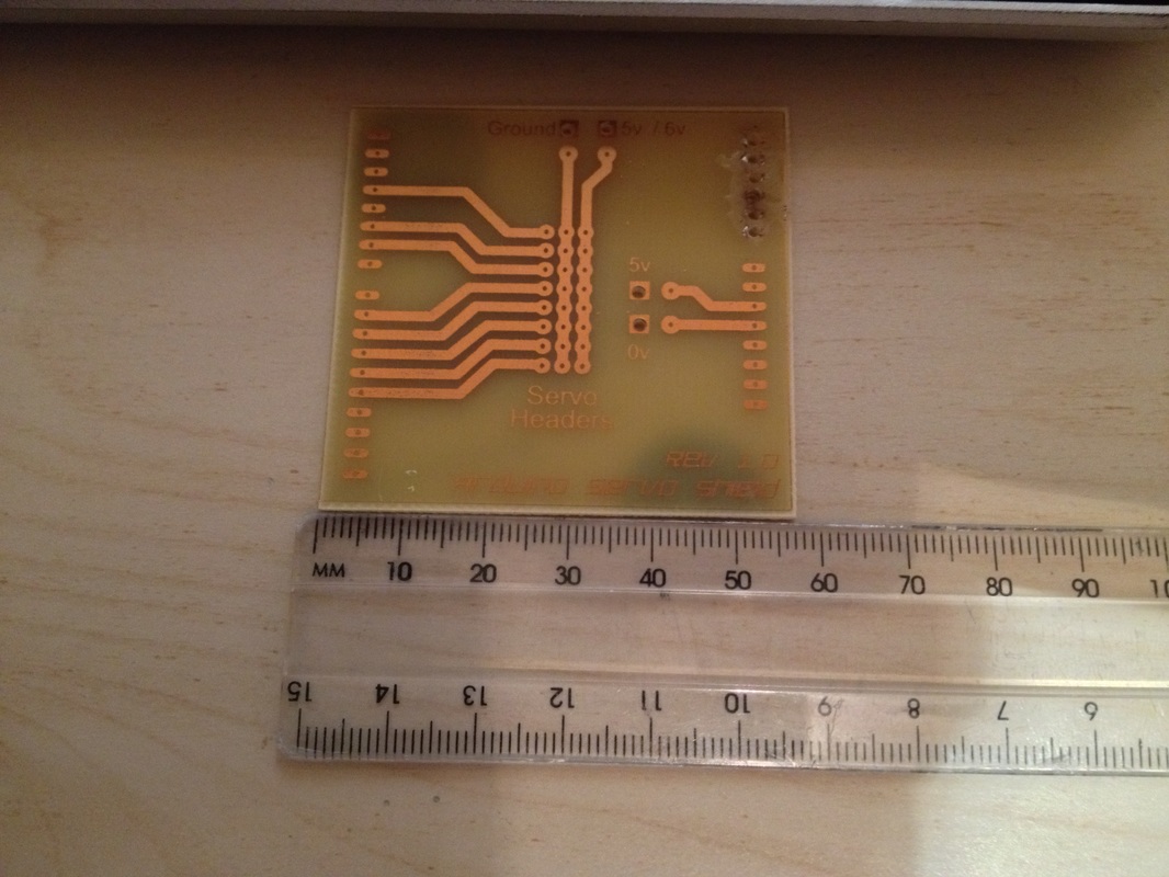
- As has always been my experience, things come out much smaller than you think they are going to be when they have been manufactured. CAD packages (Computer Aided Design) give the user the ability to zoom, this can be extremely useful but also means a gap of 2mm can look massive on the screen. If you are soldering to it by hand then you need to give yourself a big enough environment to work with! (As you can tell, I am speaking from experience a bit here!)
- This is not always the case, but sometimes a circuit board will be flipped when manufactured. You must take this into account when designing your boards, especially when they have to fit with something else!
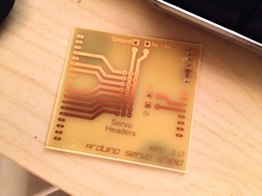
I started drilling it out already on the top right, but just ignore that as those pins are not actually connected to anything on this board, they are just there to give the board my stability when it is mounted onto the Arduino. This board is actually extremely simple when it comes to electronics, as really it's just a tidy way of making some connections. So lets run through it using the file on my Circuit Design Software.
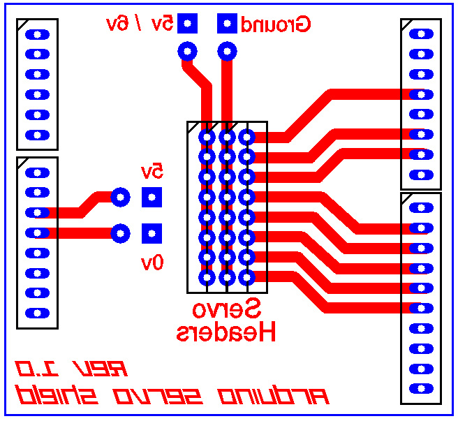
So firstly lets address the elephant in the room. WHY IS IT BACKWARDS!? Well remember what I said earlier about the board being flipped during some manufacturing processes, that is true here. My school uses a UV Box and etching tank to make the boards, so the design needs to be flipped in order to appear the right way round in the real world! It's a slight inconvenience sometimes, especially in designs like this where the way round the board is matters. But most of the time it makes little difference. Lets look at the rest of the board then:
Pads: These are the blue thingy's dotted all over this board. Pads come in my shapes and sizes and are essentially used whenever a component has to be attached to the board. These pads are designed for through hole components as they have the area with no copper in them. Blue or Red means copper! As always there are exceptions to the rule! The square shaped pads are actually "strain holes", they are designed to take the strain off of the solder joint of a wire being acting as an anchor point. The wire is looped through this hole to achieve the desired effect. Most of the pads you can see on this board are for header pins; header pins are almost like prongs designed to connect boards together.
Tracks/Traces: The red lines you can see on the board are the tracks or traces. They are designed to carry current from one place to another, like roads for electrons! Think of the M1. Any components that need connecting are done so using traces. It's important to remember that traces cannot cross, so the board has to be designed so that they can work around each other. When you really can't make the board without crossing some traces, you can use jump leads to create a bridge for one to go over the other. However we try to avoid this as much as possible!
That's mostly all simple circuit board design is, connecting pads in the right way using traces! That's why its so fun, because its like a big puzzle every time! Which way do I route the traces in order to not have to use any jump leads and make my circuit!
So what about industry, well that's a bit more advanced. Not only are the manufacturing processes bigger and better but the circuit design is also different. Not only are surface mount components commonly used (components that sit on top of the solder side rather than having leads that are pushed through holes), but boards can be double sided or have multiple layers, like stacking loads of boards on top of each other into one big sandwich! This allows more complex designs to be put onto a single board, rather than having multiple boards do the same job, saving money and manufacturing time!
I hope that gave you a bit of insight into how it all works! Keep your eyes peeled as this board will be appearing in future posts about the robot arm! (I cant wait!)
See you soon!
Sam