Many posts back I talked about FPGAs of Field Programmable Gate Arrays; if you follow me on Twitter you will know that I recently got my hands on one! So let's take a look! I thought it would be best to talk you through the hardware first, before showing you the process of programming an FPGA, in an extremely short version!
FPGA's come in many different sizes, both physically and in the size of the 'program' they can store. I write program like that because well, they are not really program's. In fact the only similair factor is that they can be written in specific languages, but more on that later. The particular FPGA I got is a Cyclone IV from Altera, specifically the EP4CE22F17C6. This chip has 154 IO Pins, 22320 Logic Elements, 608256 Memory Bits and 4 Phase Locked Loops (PLL's), as well as other stats. These are stats that I myself don't really understand; what I do know is that it is mostly the amount of logic elements that determines the amount of hardware you can fit on an FPGA. However for our purposes we should be no where near that amount! At least for the time being... :D
FPGA's come in many different sizes, both physically and in the size of the 'program' they can store. I write program like that because well, they are not really program's. In fact the only similair factor is that they can be written in specific languages, but more on that later. The particular FPGA I got is a Cyclone IV from Altera, specifically the EP4CE22F17C6. This chip has 154 IO Pins, 22320 Logic Elements, 608256 Memory Bits and 4 Phase Locked Loops (PLL's), as well as other stats. These are stats that I myself don't really understand; what I do know is that it is mostly the amount of logic elements that determines the amount of hardware you can fit on an FPGA. However for our purposes we should be no where near that amount! At least for the time being... :D
So, having the FPGA is all well and good, but we actually need a board to use it on! FPGAs are relatively picky when it comes to the environment they are in. They have to have specific infrastructure around them to operate properly. This is where the development board I purchased comes in, known as the DE0 Nano. It's job is to house the FPGA and anything it needs to operate. Most development boards also have some extra accessories such as Real Time Clocks or Display's that are wired up to the FPGA so you can use them in your projects!
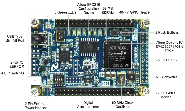
So what's on the DE0 Nano Board? Well, apart from all of the ICs required to facilitate the operation of the FPGA, there is 32MB of SDRAM, a Digital Accelerometer, a 2Kb EEPROM, 8 LEDs, 2 Push Buttons, a 4 Way DIP Switch and an Analog to Digital Converter. The LEDs and Switches will be very useful for early projects when learning about Verilog and how to program FPGA's. Things like the Accelerometer and RAM will be useful later on in more complicated projects, so exciting things to look forward to in the future! This board is also incredibly small, around the size of a debit card in fact! This makes it extremely portable and its rather amazing that they fit this much stuff into such a small form factor! So why did I choose this development board specifically? Well FPGA's are something I have been wanting to play with for a while, however they can be extremely expensive and thus can be quite a money sink if you don't end up enjoying using them. This is currently one of the best development boards on the market at a cost of £66 on Farnell, which is way better than the £100+ that some other boards cost. Coupled with the additional hardware on the board and tutorial's provided, this board is a really good deal for someone wanting to test the water with FPGAs! There are other boards out there that provide more peripherals like display's that make the FPGA easier to with external item's. But its fun and educational to hook up hardware yourself, so sometimes a slightly more bare bones device is all you need! It also helps that I'm a real hardware nerd, and this board looks really awesome!
Anyway, moving on from that. Lets get down to business and actually do something with this board! That was the point I ran into problem's nearly a month ago. The tutorial provided by Terasic (the creators of the DE0 Nano) was great for walking me through how to create, compile and upload a project in quartus (Altera, the maker of the FPGA and programming software). However, this is little use when you don't know a Hardware Description Language or HDL in the first place! Once I had completed the Terasic Beginners Guide there was little other documentation to help me learn one of the languages required to program an FPGA. Luckily, the internet was there to help me some what!
After a bit of research I decided to learn Verilog HDL, as it has similarities to C in it's syntax and thus should be a bit easier for me to pick up. It is also fairly commonly used in Industry which may come in handy in the future! Unfortunately the task of learning Verilog is a lot harder than other languages, mostly because there is little documentation out there at all that is very useful if not put in context. There are plenty of University Course Guides on the Internet, but they get way too complicated way too quickly, which just makes things confusing. However after some hard searching I found a few websites which helped me to get a foot through the door (listed at the bottom of this post), and from there it's just a matter of learning bits of syntax bit by bit. The task of learning a language is not learning all of the words or syntax that the language uses, you can find that information easily online at any point and your understanding will increase as you do projects. No, learning a language means learning it's structure and understanding how all the pieces fit together. Once you start to do this things become a lot easier!
So, lets program something in Verilog! Mostly for my own benefit this is going to be very simple, however more complicated projects will come in the future! We are going to do a very simple Multiplexer system, where we can drive four outputs with only two inputs! In this case our inputs will be the push buttons on the DE0 Nano Board and the outputs will be four of the eight LED's also on the board. Lets get started!
Stage One - Creating a Project and Setting up the Device Requirements
I am going to try and keep this tutorial somewhat generalized so that anyone can use it. One problem with some of the tutorials online was that they were very specific to hardware, so I will try to avoid that where possible. I will mention where things may differ for your hardware, in these places you should refer to your hardware manual for the information you require.
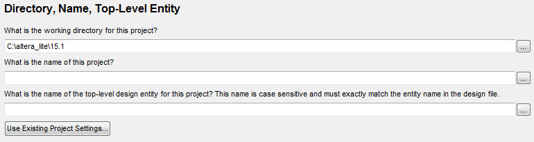
We need to start by creating a project in Quartus, in this case I am using the latest version of Quartus Prime at the time of this post (15.1). On the home splash screen of the software, you want to click the button that says "New Project Wizard", this will open up a box that guides you through the process of starting a new project. When this box opens, click next. Now you have to choose a working folder on your computer, as well as enter the name of the project in the provided boxes. Do not use a number as the first letter in your project name, so other characters are also limited but all the letters and numbers are available to use so you should have no problems. It would be a good idea to name the working folder as the same name as the project, just for ease of use later on.
So what's on the DE0 Nano Board? Well, apart from all of the ICs required to facilitate the operation of the FPGA, there is 32MB of SDRAM, a Digital Accelerometer, a 2Kb EEPROM, 8 LEDs, 2 Push Buttons, a 4 Way DIP Switch and an Analog to Digital Converter. The LEDs and Switches will be very useful for early projects when learning about Verilog and how to program FPGA's. Things like the Accelerometer and RAM will be useful later on in more complicated projects, so exciting things to look forward to in the future! This board is also incredibly small, around the size of a debit card in fact! This makes it extremely portable and its rather amazing that they fit this much stuff into such a small form factor! So why did I choose this development board specifically? Well FPGA's are something I have been wanting to play with for a while, however they can be extremely expensive and thus can be quite a money sink if you don't end up enjoying using them. This is currently one of the best development boards on the market at a cost of £66 on Farnell, which is way better than the £100+ that some other boards cost. Coupled with the additional hardware on the board and tutorial's provided, this board is a really good deal for someone wanting to test the water with FPGAs! There are other boards out there that provide more peripherals like display's that make the FPGA easier to with external item's. But its fun and educational to hook up hardware yourself, so sometimes a slightly more bare bones device is all you need! It also helps that I'm a real hardware nerd, and this board looks really awesome!
Anyway, moving on from that. Lets get down to business and actually do something with this board! That was the point I ran into problem's nearly a month ago. The tutorial provided by Terasic (the creators of the DE0 Nano) was great for walking me through how to create, compile and upload a project in quartus (Altera, the maker of the FPGA and programming software). However, this is little use when you don't know a Hardware Description Language or HDL in the first place! Once I had completed the Terasic Beginners Guide there was little other documentation to help me learn one of the languages required to program an FPGA. Luckily, the internet was there to help me some what!
After a bit of research I decided to learn Verilog HDL, as it has similarities to C in it's syntax and thus should be a bit easier for me to pick up. It is also fairly commonly used in Industry which may come in handy in the future! Unfortunately the task of learning Verilog is a lot harder than other languages, mostly because there is little documentation out there at all that is very useful if not put in context. There are plenty of University Course Guides on the Internet, but they get way too complicated way too quickly, which just makes things confusing. However after some hard searching I found a few websites which helped me to get a foot through the door (listed at the bottom of this post), and from there it's just a matter of learning bits of syntax bit by bit. The task of learning a language is not learning all of the words or syntax that the language uses, you can find that information easily online at any point and your understanding will increase as you do projects. No, learning a language means learning it's structure and understanding how all the pieces fit together. Once you start to do this things become a lot easier!
So, lets program something in Verilog! Mostly for my own benefit this is going to be very simple, however more complicated projects will come in the future! We are going to do a very simple Multiplexer system, where we can drive four outputs with only two inputs! In this case our inputs will be the push buttons on the DE0 Nano Board and the outputs will be four of the eight LED's also on the board. Lets get started!
Stage One - Creating a Project and Setting up the Device Requirements
I am going to try and keep this tutorial somewhat generalized so that anyone can use it. One problem with some of the tutorials online was that they were very specific to hardware, so I will try to avoid that where possible. I will mention where things may differ for your hardware, in these places you should refer to your hardware manual for the information you require.
We need to start by creating a project in Quartus, in this case I am using the latest version of Quartus Prime at the time of this post (15.1). On the home splash screen of the software, you want to click the button that says "New Project Wizard", this will open up a box that guides you through the process of starting a new project. When this box opens, click next. Now you have to choose a working folder on your computer, as well as enter the name of the project in the provided boxes. Do not use a number as the first letter in your project name, so other characters are also limited but all the letters and numbers are available to use so you should have no problems. It would be a good idea to name the working folder as the same name as the project, just for ease of use later on.
Click next three times when your done entering this information. You should now be on a page that looks like this!
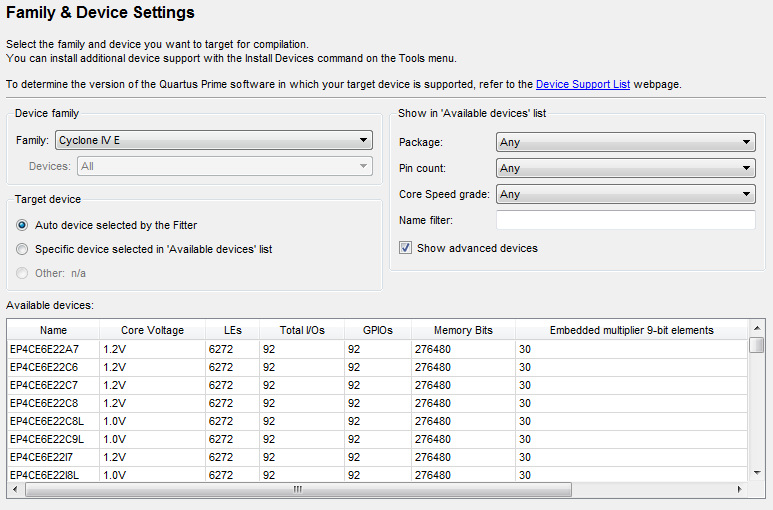
On this page you need to tell Quartus the specific Altera chip that you are using, in my case it's the EP4CE22F17C6. Check the box that says "Specific device selected in 'Available devices' list" and then use the "Name filter" box to search for your specific device. When you find it just click on it to highlight it, then click next! On the next page there will be a column that says format's. Change the box that says VHDL to Verilog HDL and then click next! Finally click finish and Quartus will create your project!
You should be met with a blank screen at this point. Firstly you need to create a new Block Diagram file. Click the new file icon in the top left hand corner and then select Block Diagram in the list. A Block Diagram is basically the schematic of the hardware that will be implemented on your FPGA. You should save this file once it is created, making sure you name it exactly the same as your project name. Doing this means that Quartus will default this file as the top level design entity, which is exactly what we want. This file is essentially where all the different modules we create are connected together, much like the schematic for a circuit board. We will be doing more in this file later, but for now just leave it alone... :D
Now that this file is created we need to make the Verilog File that will house the code for our Multiplexer Module. Again go to the top left hand corner and click the new file icon, however this time in the file type list select Verilog HDL File. A text editor will open up, this is where you type your Verilog Code that will make up the Multiplexer Module. You may have noticed I keep saying "Module," well before we look at the Verilog Code for the multiplexer we need to talk a tiny bit about the structure of Verilog.
Verilog is entirely made up of things called Modules, they are like descriptions of specific bits or sections of hardware. For example you might have a module that describes a shift register for use in a UART. All Verilog code needs to be contained within a module, these modules can then be instantiated elsewhere in the code with specific input values, much like functions in C. The idea is that you write the individual modules, and then instantiate versions of them in the correct connected layout to make your overall hardware design. Whether that be a completely custom chip or your interpretation of a specific processor package. I will go more into the ins and outs of Verilog in a later post, but I thought it best we understand how to program our FPGA first before we learn to code in the language.
So lets have a look at out Verilog Code! Here it is:
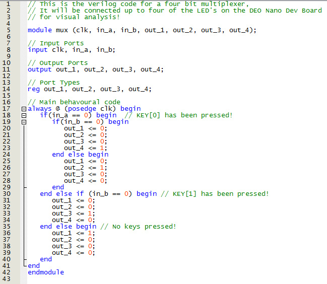
AHHHHH! Lots of extremely confusing code, help! Lets break it down, you will find that it makes a lot of sense once you understand each bit. It is extremely important to remember that we are not programming a Microcontroller here. Our aim is to describe a piece of hardware, so that means describing the states of it's output's when it's inputs are in certain states.
Line number 5 is creating out initial module. We are not instantiating a module here, but rather creating a new one, much like we would create a new function in C. The variables in the brackets are the names of all of the ports that will make up this module. At this stage we are not defining whether they are inputs or outputs, we are just saying that they exist.
Line number 6 is used to declare which of the ports are inputs, in this case we have three inputs: clk, in_a and in_b. Much like line 6, line 11 is devoted to declaring which ports are outputs.
Line number 14 is used to declare the types of ports that we are using, this is where it gets a bit more complicated. The syntax that says "reg" is short for "register." This means any port that acts like a register, in other words it stores the value that was last inputted too it. You may have noticed that I have not declared the type of every port in the module here! Any port that has not got a declared type defaults to type wire. The wire type does what it says on the tin, it acts like a simple wire that needs to be driven to be a certain value. In other words it does not retain it's last inputted value like a register, it must be constantly driven at that value.
Line number 17 is where the meat of the code starts. This is the main behavioral section of the code, or in other words the part that describes how the module will react to certain inputs. We must always start by telling the system at what point it should check the value of the inputs, in this case we are checking the inputs and changing the outputs accordingly on the rising edge of the clock. This is why we are using the phrase "always @ (posedge clk) begin." What follows is much like what you would see in some simple C code, where we tell the system how it has to react to certain input states. You will notice this strange looking symbol: "<=". For now all you need to know is that this is setting the variable to the value on the right hand side of the symbol.
Finally, whenever we start a specific section of behavioral code, whether that be an if else statement or an always @ statement, we must put in "begin" and "end" to tell the system where this little snippet of code starts and ends. Much like the } in C! So that's out Verilog Code done, what next? Well we need to make a symbol file for this module so that we can but it into out schematic file!
Go to File, Create/Update and click on "Create Symbol Files for Current File," if all foes according to plan this will complete successfully. Now switch to the schematic file and double click the dotted area where you draw the schematic! A boc will come up that looks like this:
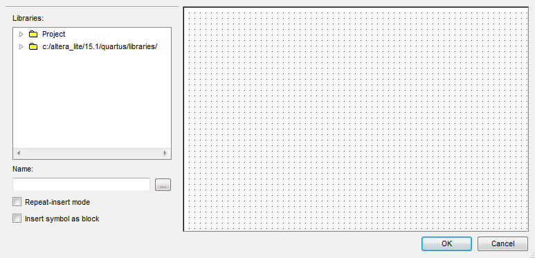
Click on the Project drop down file and then click on the name of the module we created in our Verilog Code, then click ok. At this point the schematic image of the module we created in Verilog Code will move around with your mouse. Click to place it down onto the schematic. We now need to add a few more things to our schematic that are required for this hardware to run properly!
Firstly we need to add something called a Phase Locked Loop or PLL. This is essentially a section of hardware that converts an input clock signal to a different frequency. In this case the DE0 Nano has a 50Mhz input clock signal, which we will then convert to 5Mhz. As far as I know we don't technically need to do this, but it is good understanding to gain now as it will be very useful later on! So lets make our PLL!
If the IP Catalog is not open on the right hand side of the screen then click the tools header and select IP Catalog in the drop down menu! Once this is open select Library, Basic Functions, Clocks; PLLs and Resets, PLL, ALTPLL. Then click "Add.." at the bottom of the IP Catalog. A window that looks like this will open up!
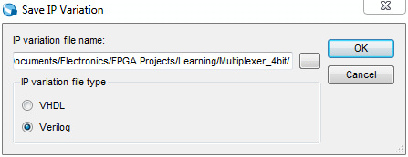
Enter in the text "pll.v" at the end of the file name box. Then make sure Verilog is selected and press "OK." A window like this will open up:
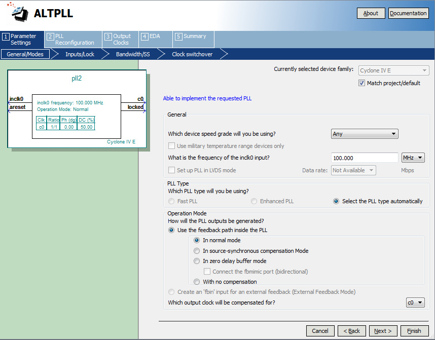
Change the box next to "What is the frequency of the inclk0 input?" to 50. This is because the main crystal of our system has a 50Mhz frequency as I said earlier. Press Next. On this page uncheck any boxes that are checked and then press next four times! You are now looking at the output clock section of the module creator, this is where we declare the frequency of the output clock that we want the PLL to provide. The page should look something like this:
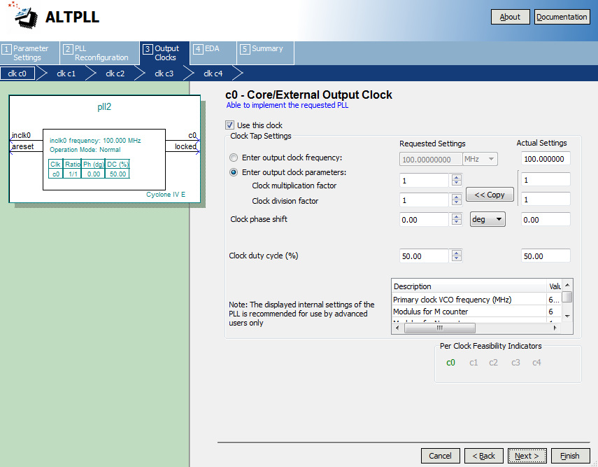
We need to set the box next to clock division factor to 10, as we want an output frequency of 5Mhz! Once you have done this click next six times! You will now be on the final page! All we need to do now is check the box next to the .bsf file, this will generate the symbol file for the schematic later on! Once this is done click finish!
Now we need to make our schematic! This is the top level of the design that brings all of the modules we have created together! When we are finished it will look something like this!
Now we need to make our schematic! This is the top level of the design that brings all of the modules we have created together! When we are finished it will look something like this!
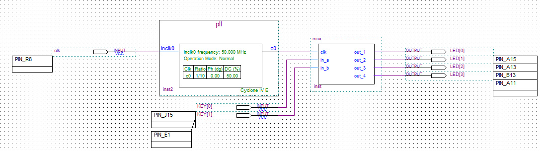
Firstly we need to add our PLL, the module that we just created using the IP catalog! Double click on the schematic area, go under project and select the PLL, then click ok! Place the PLL into the schematic where it is in the image above! Connect it up to the Multiplexer Module as you can see above! To connect pins, click on the pin of one module and drag to the pin of the module you want to connect it to! Finally we need to add our input and output pins! Double click on the schematic screen again, the input and output pin parts can be found here:
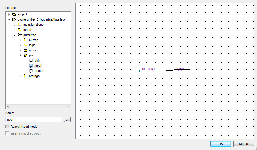
Add in input and output pins as they are in the diagram above, you can double click on the pin part to change it's name! Once this is done we are ready to go into the pin planner and tell the system which input and output parts on the schematic link to which physical pins on the FPGA! Before we do this, click the play button at the top that has a green tick in it, it should be label "start analysis and elaboration" when you hover over it. If this passes the there is nothing wrong with what you have done so far!
To open the pin planner go to assignments on the top bar and select the "pin planner" option. When you are done this screen should look like this!
To open the pin planner go to assignments on the top bar and select the "pin planner" option. When you are done this screen should look like this!
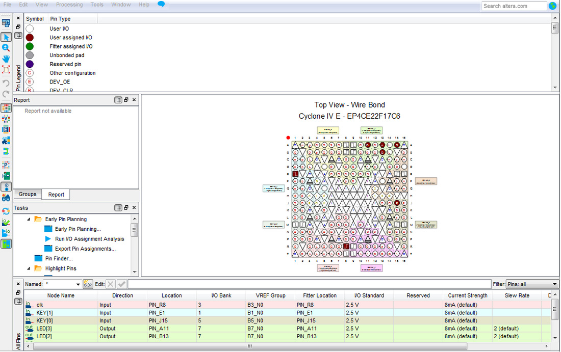
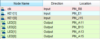
All we need to do on this page is fill in the table below the diagram of the FPGA, I know this looks a little confusing but bare with me! To fill in the table correctly you need to type in the correct pin name next to the correct schematic part. This is why it is helpful to label your parts in the schematic, as it is much easier to see what is what at this stage! You will need to check for your specific hardware, but for the DE0 Nano the pin assignments for this project are as follows:
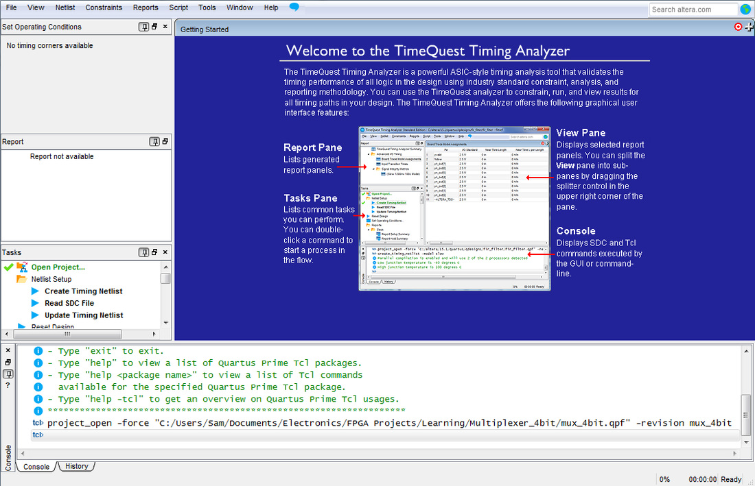
Once this is completed simply close the pin planner! We now need to tell the system the generic timing constraints for this system. The concept of this is extremely confusing, I don't really get it at the moment either! But for our purposes we can get through this step fairly easily. Go to tools in the top bar and select "Timequest Timing Analyser," this will open up a screen that looks like this:
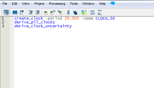
Go to file and then "new SDC file." This will bring up another text editor where we must enter the timing constraints for this system. Copy the text that you can see in the image below!
Once this is done press file and save as, making sure that you save the file with the same name as the project. This will automatically link this timing file to the project, meaning you don't have to do this step manually! Now this is done, we are ready to compile and upload this code to our development board! There is one extra step we could do where we would virtually test the code, but I will look at this in a later blog post! This technique is used a lot in industry to save time and money.
Finally click this button at the top of the main window!
Finally click this button at the top of the main window!

This will start the compilation of all of the files you have created into one "sof" file. This is the file that we can upload to our development board and test! Once this has completed go to tools and then programmer! There are a few things we need to do here before we upload our code to our system. You should see a screen like this:
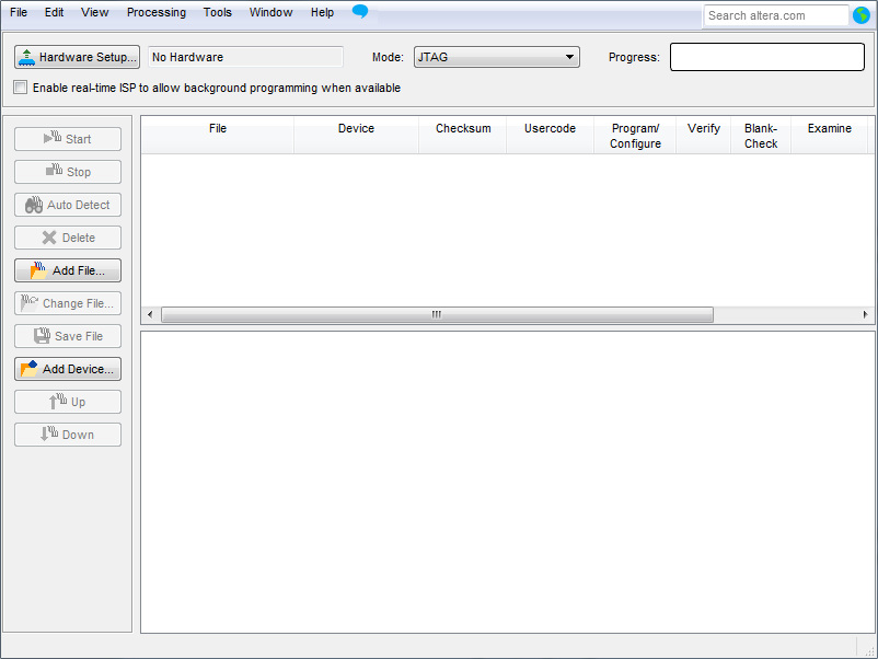
First click the "Hardware Setup" button at the top and make sure the that your device is selected in the drop down box! It should say something like "USB Blaster [0]." Then we need to add our ".sof" file! Click the add file button on the left and navigate to the ".sof" file. It is usually in a folder labelled output files. Once this is not, click the start button in the top left, once the progress bar hits 100% your FPGA is programmed and it should be acting as a simple decoder/multiplexer! Congratulations, you have just completed a project using the Altera Quartus software! It took a bit, but we made it to a great result in the end, even if it doesn't really do an awful lot!
A few things of note with this guide:
Sam
A few things of note with this guide:
- This tutorial only works with the Altera Quartus Software, which is subsequently only for use with the Altera line of FPGA's. If you have an FPGA from Xilinix or another company then there are plenty of tutorials online on how to use their software, just search "FPGA tutorial Xilinix!"
- If you unplug and plug back in your FPGA the hardware will no longer be on the system. This is because the FPGA stores the hardware information in volatile memory, which is cleared when the power is removed. The DE0 Nano Board has a simple way of permanently storing the setup information. I'll talk about this in a later post!
Sam
